
New building blocks expand functions of photonic chips
With integration of single-crystal nanomembranes, WashU engineers establish a framework for photonic circuits
Most of today's computer chips – also sometimes known as conventional integrated circuits – use electrons to deliver their signals via semiconductor materials and metallic components. In contrast, photonic integrated circuits use faster signal carriers, such as photons or quantized ‘light particles.’
Over the past decades, many academic and industry researchers have looked for ways to integrate photonic materials onto chips. By enabling optical links that move data at high speed, these researchers seek to make new kinds of chips for artificial intelligence (AI) systems, photonic computing, co-packaged optics (CPO) and new approaches to sensing and quantum technologies.
However, getting the desired high-quality materials needed to integrate photonics into chip architecture has been the challenge, a challenge that researchers at the McKelvey School of Engineering at Washington University in St. Louis have started to solve.
“We developed a manufacturing process that will give us more freedom to design these new photonic chips,” said Sang-Hoon Bae, assistant professor of mechanical engineering & materials science at McKelvey. Bae is co-corresponding author of research now published in Nature, about a modular materials framework for multifunctional photonic circuits.
Bae’s colleague at McKelvey, Lan Yang, the Edwin H. & Florence G. Skinner Professor in the Preston M. Green Department of Electrical & Systems Engineering is co-lead investigator on the project with profound expertise in integrated photonics. Bae first approached joining WashU with this collaboration in mind with Yang. It’s taken years of work, but the team has found the right process and materials to add new capabilities to photonic chips through heterogeneous integration.
“Silicon photonics gives us a powerful foundation, with decades of investment in chip fabrication and design,” Yang said. “Heterogeneous integration lets us build on that foundation while adding materials that can control and detect light in ways silicon alone cannot. That is essential to expanding what integrated photonics can do.”
“Using photons for all the best chips is one of the most interesting and fascinating directions for the industry,” Bae said, adding that the challenge has been finding ideal materials that can integrate with current chip architecture while maximizing photonic integration.
In the new research, the team details how they developed materials and showcase the framework’s use on the photonics side, he added.
“We demonstrate much faster modulation, efficient isolation, we also showcase wide-spectrum light detection, with a full functionality package,” he said.
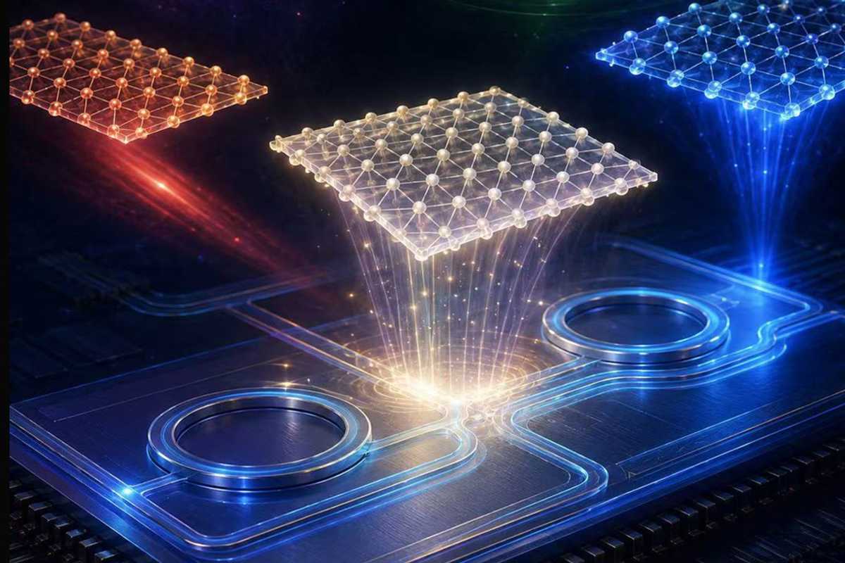
The framework brings new functions and capabilities to established silicon and silicon-nitride photonic chips by transferring ultrathin, freestanding single-crystalline nanomembranes onto prefabricated optical circuits.
The WashU researchers avoided known constraints for materials grown directly onto silicon by developing a veritable buffet of ultra-thin films that can be placed directly where their diverse properties – including electrical, magnetic or optical properties – are needed. The framework functions like photonic Legos, giving tech developers many more options in building the circuits that power the modern world.
“Each material brings its own strengths,” Yang said. “By growing high-quality crystals separately and then bringing them onto an existing photonic circuit, we gain more freedom to choose the material for the function we need. We can also combine materials side by side or stack them to bring several functions into one device.”
For example:
- Single-crystalline barium titanate (BTO) nanomembranes enable highly efficient electro-optic modulation.
- Cobalt ferrite (CFO) nanomembranes bring nonreciprocal light control to their set of tools.
- Gallium arsenide and gallium nitride membranes were laterally integrated on silicon nitride to detect light at selected wavelengths, from the ultraviolet to the near-infrared, using different devices on the same chip.
- Stacked barium titanate and cobalt ferrite on silicon micro-ring resonators combine electro-optic and magneto-optic functions for multifunctional photonic applications.
And, this is just the start. Having a way to bring different functional materials onto the same platform, it opens the door to many more choices in how photonic systems are designed. The opportunity is to build different combinations of materials around the needs of each application.
Meng Y et al. Heterogeneous photonic integration of single-crystalline nanomembranes. Nature 657, 638–645 (2026). DOI: https://doi.org/10.1038/s41586-026-11000-w
This work was supported by National Science Foundation (NSF) Program-EPMD (2428676) and McKelvey Collaboration Initiation Grant (WashU CIG) to Sang-Hoon Bae and Lan Yang, who are co-corresponding authors of the paper. Sang-Hoon Bae acknowledges funding support from NSF (2240995, 2329189) and Air Force Research Laboratory (AFOSR) (FA9550-25-1-0321). WashU Postdoctoral Research Associates Yuan Meng, Wenbo Mao, PhD student Zhihao Xu, and postdoc Di Jia are the co-first authors for this Nature paper.
The experiments were supported by the facilities of the Institute of Materials Science and Engineering (IMSE) at WashU and partly by the Holonyak Micro & Nanotechnology Lab (HMNTL) at the University of Illinois Urbana-Champaign (UIUC).